PICTURES
Here's the pictures related to CopyNES, with a description for each. Click on the picture for a larger view.

CopyNES' Front Panel
This is the front of CopyNES. The only changes that are visible is the addition of an LCD display showing the unit's status, and the nice bright
yellow LED for power. Note I left the controller connectors out... this is because I forgot where I put them and couldn't find them for the pictures!!

Closeup of the LCD display
Here's a closeup of the LCD.
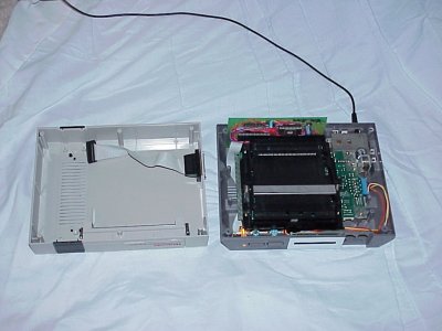
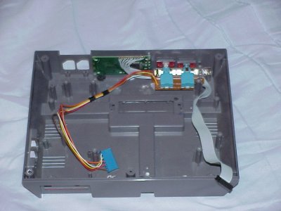
The Guts
Inside the unit, the actual CopyNES add-on board sits behind the black cartridge connector, and is connected to the NES CPU board via a 34 pin ribbon cable (not visible). The 14 pin ribbon cable that is visible snaking around the side of the cartridge port goes to the LCD display on the front. On the left, the DB25 connector that runs to CopyNES' board can be seen screwed to the side. It terminates in a 26 pin IDC connector (I stole this off an old motherboard :-).

Backside of the Unit
To make the board stay put in the NES, I cut a slot in the bottom of the case, where the wire ridge is at. The perfboard then sits down in this channel. A piece of wire acts as a detent to make sure the board stays put. The board is tall enough that the top of the case will keep it down in the channel. It cannot move side to side both because of the tightness of the fit, and because the 34 pin ribbon cable. There is enough play in the ribbon cable however to allow the board to be pulled up and out and the connector can be removed and installed without too much hassle.
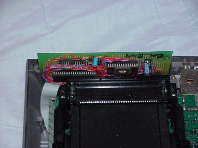
Front of the Board, Installed
CopyNES' perfboard can be seen resting in the afore-mentioned channel nestled behind the cartridge port's connector. The 14 pin ribbon cable can be seen a bit better here, plugged into the board with an IDC connector. The 26 pin connector near the top of the board goes to the DB25 port which is mounted to the top half of the NES case.
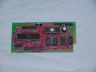
Top of the Add-On Board
On the top of the add-on board, all 6 chips are visible. They are (left to right):
 6522 Port chip. Does all I/O to the host computer and LCD display, as well as copy/play mode control. 6522 Port chip. Does all I/O to the host computer and LCD display, as well as copy/play mode control.
2764 (windowed part at the top). This holds the 8K of control code.
7410, 7432, 74157, 74138. This is the misc. "glue" logic.
At the top, the 26 pin connector is visible, which connects to the DB25 parallel port connector. On the lower-left is the 14 pin connector for the LCD display which is mounted to the front of the unit. And at the bottom is the 34 pin connector that plugs into the CPU adaptor. The large capacitor at the top, as well as the slide switch are for the EPROM emulator. (The cap is there 'cause the emulator's bypassing sucks, and the switch is there because it thinks that pin 27 is an address line; which needs to be pulled high for EPROMs and hence pulled low for the emulator.)
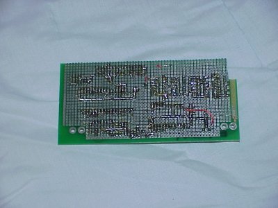
Solder Side of the Board
Not much to say here... solder side of the above board. The resistor hanging on at the right is for that afore-mentioned switch. It was a quick hack to get the emulator working.
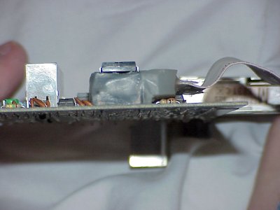
Inside View of the Bottom Half
The LCD is mounted to the back of the front side using 2 flathead screws in countersunk holes, so that when the laminate was placed over the top, they would not be seen. The cable from the LCD is snaked below the switch assembly to make sure it clears the cartridge mechanism (note: this is pretty tricky! be sure to test your mechanism while/before you install the LCD). I snapped off the support column since it would not clear the LCD. This support is not really required since the other screws hold the case together well enough.

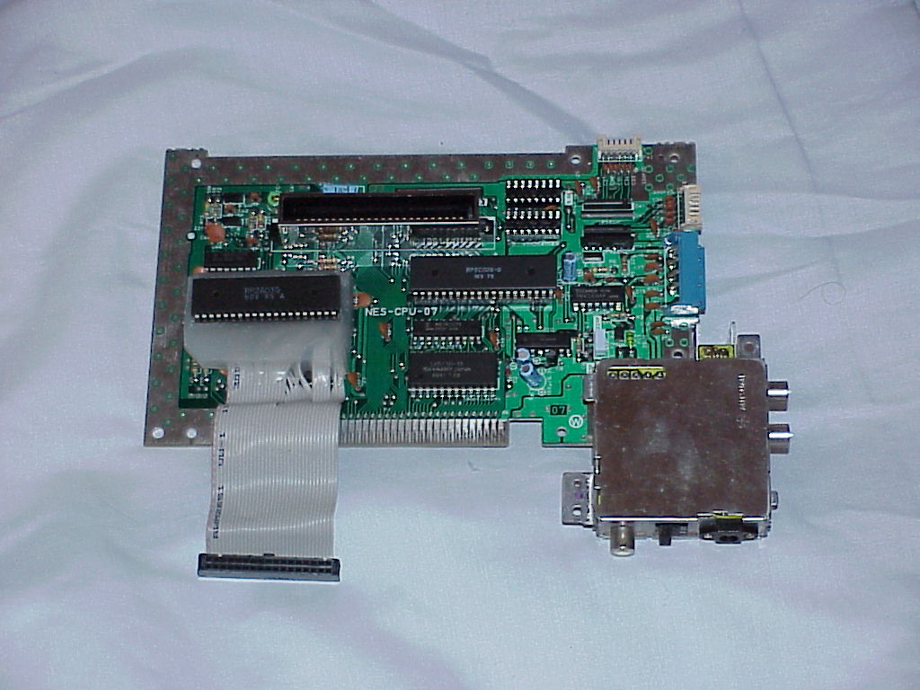
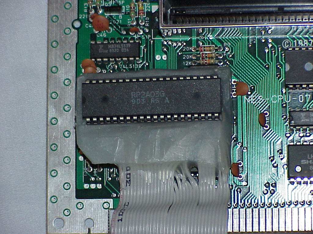
The Modified NES CPU Board
CopyNES' CPU socket/adaptor is soldered directly to the board, where the CPU originally sat. The CPU is then plugged into the top of it. The 34 pin ribbon cable then connects to the add-on board. Note that this is the trickiest part of the whole unit. Make sure that your socket clears the RAM chip next to the CPU!! I had to slice some of the hot-melt off with a razor to make it fit. Also, do not make the socket any higher than a normal socket soldered to the top of an IDC connector (bottom half only) since once the CPU is installed, it will not fit back in the case. I originally wanted to have the CPU adaptor socketed, but this was not to be. Note that the joypad controller chips are missing (sockets only) and the PPU is also socketed. This is because I had an umm, "event", shall we say relating to the power switch assembly. Do not let this dangle when the NES is plugged in! It dangled onto the main board when I was assembling it (with power plugged in but the NES switched off) and blew up those 3 socketed chips, the EPROM, and the port chip! You have been warned :-).

Socket Closeup
The ribbon cable can be seen exiting the hot-melt. Note that the wires all don't exit cleanly- this is because they are going every which way after being soldered to the pins of the socket.
Side of the Socket
And finally, a shot of the side of the socket showing the cable exit, cut out portion to fit the RAM, and my feet :-) (holding the board upright to take the pic).
|