Building the PSS CPU module clone
|
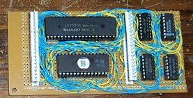
After I unpotted the CPU module, I decided I should make a clone of it to verify my ROM dump and circuit, and just prove it was indeed possible. Now that the circuit has been figured out, I can look back on it to see all the tricks they devised to make it difficult to dump the ROMs.
The ProtectionThe protection consists of several ingenious things that they did to make life difficult. First, there is an execution protection that prevents code above 8000h reading the data at 0000-7FFFh. This is accomplished with the use of a flipflop and some gating. It uses /M1 out of the Z80 and /MEMREQ to detect the opcode fetch. When the opcode fetch occurs, it latches the state of A15. If A15 was 0, then the ROM will be "unlocked". If A15 was 1, the ROM is then "locked". Any form of I/O access will also reset the flipflop and lock out the ROM. The other method of protection used is to buffer the /RD and /WR signals so that they cannot be forced high/low externally, and A14 and A15 do not leave the block, which makes it impossible to force them high/low either. A14 and A15 are used to do all address decoding for the memory mapped devices.
The SolutionThere are several methods of attack possible to dump the ROM data.
Method #1:
Method #2:
Method #3: LD A,(HL) RET Once some suitable code is found, it is then possible to use this load instruction to dump the ROM data using a loop in the ROM mapped in at C000-FFFF. I performed this hack to verify the dump. Whoever wrote the code was very careful to prevent ANY load instruction from memory followed by an RET. I did not find a single instance of this in the code block itself. It was always followed by some form of processing, or a conditional return after a compare operation. This might produce some useful results, but nothing easy or definite. I did manage to find the following code, however. It is part of the text to speech dictionary data and just happened to be usable... 1a39 4e ld c,(hl) 1a3a 41 ld b,c 1a3b 5f ld e,a 1a3c 95 sub l 1a3d 80 add a,b 1a3e a9 xor c 1a3f 1f rra 1a40 8b adc a,e 1a41 c9 ret This unholy mess of code was just what I needed. The LD C,(HL) instruction is what I'm looking for, while the other instructions are just crap. C does not get modified by the crap instructions, however, which is good enough for me. I call this address from my dumper code and use it to dump the ROM contents out. There is a loop and some code that uses the on-board hardware (UART and counter/timer chip). It simply spits the data out the serial port where I can suction it off with a terminal program! This method was used to verify the data integrity.
Method #4: Since there is nothing mapped in at 4000-7FFFh, this part of memory will read as "open bus". Open bus is the term I use for parts of an address space that do not have anything mapped in them. No ROMs no RAMs, no nothing. Reading these parts of memory will return junk or whatever was on the data bus last. All chips on the bus will be tri-stated, leaving the bus in a high impedance state. So... what we do is solder 8 resistors on the 8 data lines... Some are soldered to ground and others are soldered to VCC. The pattern of resistors will determine what value we read for any open bus access... if the resistor is soldered to VCC, we will always read a 1. If it is soldered to ground, we will always read a 0. If we read some implemented part of the address space, (i.e. ROM or RAM) the chip will "overpower" the resistors and we will read what we want. The trick here is to set the resistors up to form the LD A,(HL) instruction. This instruction is encoded as 0111 1110b. This means that we solder resistors from D0 and D7 to ground, and resistors from D1 thru D6 to VCC. This will encode the opcode LD A,(HL). Next, we write 0C9h into location 8000h which is the start of RAM. This is the opcode for the RET instruction. Finally, we do a CALL to 07FFFh. This then runs our LD A,(HL) instruction, then the PC increments to 8000h and runs our RET instruction in RAM! A15 will be a 0 when we execute the instruction at 7FFFh, meaning we can then dump the ROM! This is then used in our loop to dump out all the data in the potted ROMs without having to open or damage anything.
Making the clone boardHere's my little picture essay of the clone board assembly.
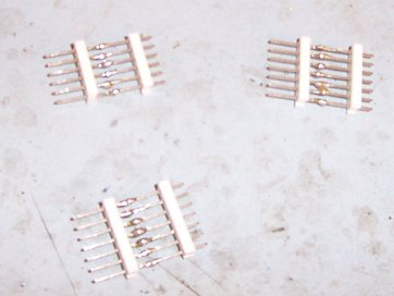
First, I made some headers up to connect my new board with the main board on the PSS. I didn't have any long enough, so I soldered two end to end to get the length needed.

Yep, the headers fit into the sockets just fine.
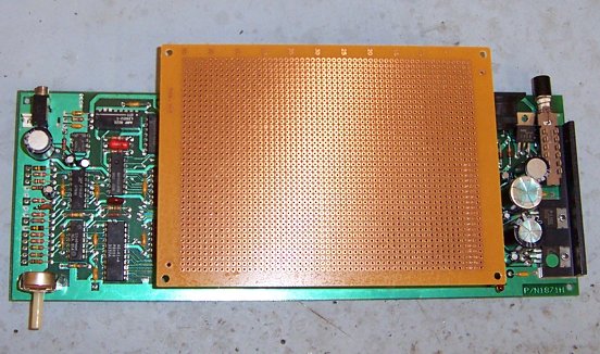
Testing the fit of the perfboard. The maximum height of the board I could allow was the top of the filter capacitors. The board is juuust a tad lower than them so it's good.
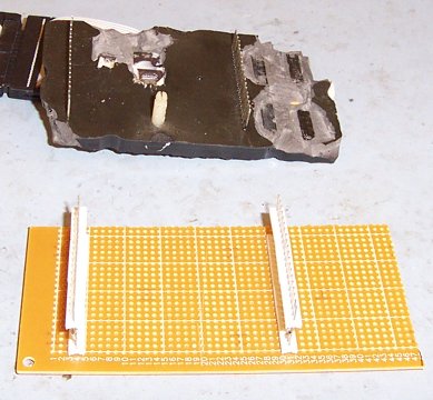
Here I have soldered the headers on and cut the board to size. It is now approximately the same outside dimensions as the potted module.
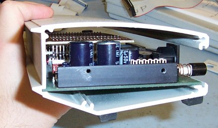
Checking fit inside the case. Looks like it fits inside pretty nicely. The board does not hit the top of the case.

I have now soldered down some IC sockets and populated them with the proper chips.
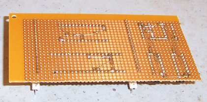
...and connected up most of the power and ground connections.

And, here is a shot of the finished clone board next to the real thing. I used a single 16K EPROM instead of the two 8K chips they used. Also, in this shot you can see I replaced the Z80 with an NMOS one. The CMOS Z80 does not work here for some reason. I can't quite figure out why this is. The NMOS one however works just fine.

Bottom view of same.
|
