Unpotting the Type N Talk
I laugh at your software security!
|

I won't go over the basics of de-potting again... If you wish to know how it is done, check out THIS page. Inside this black blob of sin, I found a 6802 microprocessor, a 4K PROM/ROM memory device, and a 7442 1 of 10 decoder which is being used to decode addresses for the other chips on the board. I was highly amused at how they glued plastic covers onto the PCB and then dumped the potting compound into it from the top... This must've taken FOREVER to do. It took me around 2 hours to totally depot (and clean) the PCB, and to dump the ROM. It probably took more time to cure than to depot :-) This device is about as simple as it could possibly be. The memory map is also very simple. A15 on the CPU is not used at all, so they mapped everything into a 32K address space. The first 8K holds the 1K of RAM, second 8K is the UART, third 8K is the SC-01, and the final 8K holds the 4K of ROM. As for the ROM, it's unknown what it is exactly... I suspect it's a mask ROM and not a PROM, but I guess it COULD be a PROM. The part was made by Signetics, which is known for making PROMs, but the part number is CN49752J. This smells like a custom marking. Inside the ROM is 4K of code which does the usual T2S algo and a very small exception table I assume.

The board fresh out of the case. The plastic potting "over-shell" is visible, filled with epoxy.

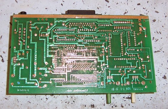
The bottom side looks very similar.
Those plastic over-shells were the first thing to go. They were kinda cute in their construction- I could not just remove them, since they had a plastic "foot" that went slightly UNDER the epoxy! I just sliced it with the x-acto knife and went to town with a screwdriver to break 'em apart.
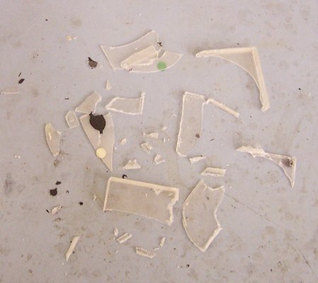
This is what we got to work with on the top. A fairly thin lump of black epoxy.
The bottom looks nearly identical.
Half-done removing the potting from the bottom. This side is fairly easy to work on. The routes are quite large, and there is a soldermask. The soldermask sticks to the epoxy but not to the route very well so it comes out easily, without damaging anything.
I always depot the bottom first, since you can then tell what parts are present by their pins. Chips are easily visible, as are any small passives. Now that the bottom is completely clear, it's time to start on the top, now that we have a "map".
I like to then remove the epoxy down to the top of the chips so we can see what the part numbers are, in case they get rubbed off or abraded. In this case, we have a ROM of some sort, a 6802 CPU, and a 7442 decoder.

Because it is at the bottom and most accessable, the CPU is the first thing to go. I removed the potting down to the pins on the front of the chip so that there was an air gap between the pin/PCB. Then, I desoldered these pins and bent the chip up carefully. This lets the air get to the other row of pins, allowing the desoldering tool to suck the solder out effectively. The CPU is replaceable... the board ain't. Note the flakes of epoxy on the table. Lots of this "swarf" is produced when depotting!

The CPU's popped out.

Now that the CPU has been removed, it's time to go after the decoder. It's smaller than the ROM, and is covering up the end of the ROM which is kind of making life difficult.
There. The decoder was removed, and the ROM is now the only thing left. All the epoxy was carefully cleaned from around the ends so that a knife or screwdriver could carefully be placed under it to do some prying after the solder was removed.

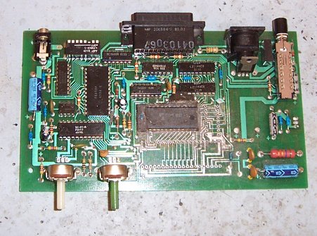
The results: I went over the PCB after all the chips were removed with some epoxy stripper to clean the board up. I think it looks pretty good after being coated with epoxy! In this pic you can see the two jumper wires I added to the board which rewires it to accept the 2732 EPROM. These wires are under the socket, so they aren't visible.
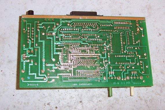
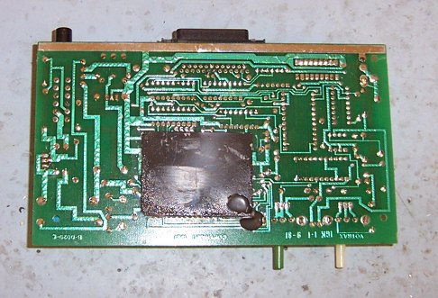
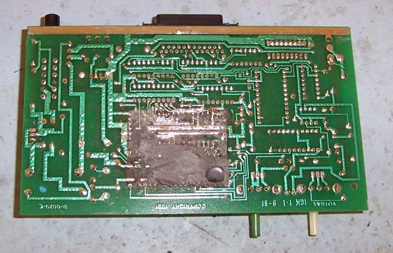
The bottom got the same treatment, too.
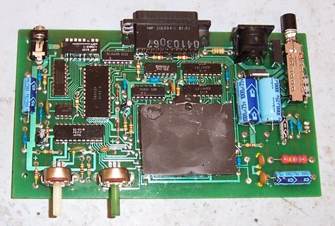
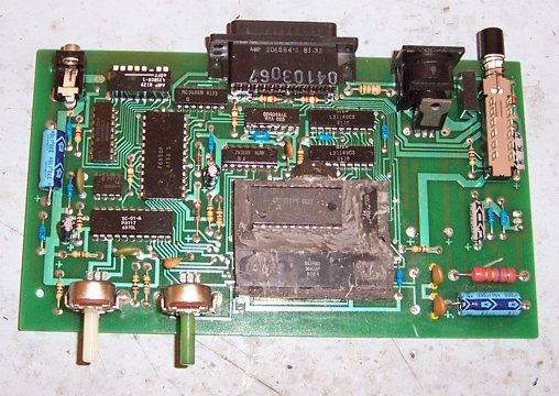
And here's the final result with the 3 sockets in place, and two chips plugged in. I thought I had a 6802 kicking around, but I don't. I'll have to pick one up before I can try this board out.
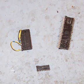
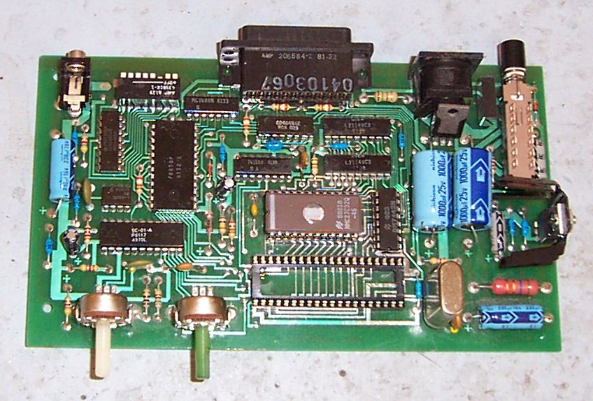
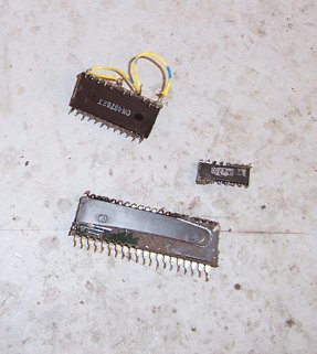
As can be seen on the ROM, I added some wires to it so that it'd match the 2732 pinout. This allowed dumping it with my EPROM programmer. There's still some potting compound on the chips; no need to clean it off if I won't be re-using them.
Bottom view.
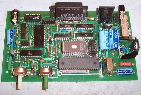
And there's the finished dealie. All the chips are installed!
|
