1,000,000 in 1 Multicart
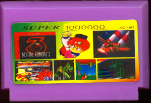
Cartridge Front


Cartridge PCB
What Is It?
This is an intresting multicart, simply because it claims to have 1 Million games on it. Nothing could be farther from the truth,
of course. In actuality there's 15 games and a clever menu arrangement that shows 1 million entries.
Note that the "1,000,000" is pasted over top of the label.
The Games:
Notables are "Mortal Kombat 3" and "Streetfighter 12 Peoples".
The other 13 games are "Multicart Fodder" titles such as Super Mario Bros and other
NROM (Mapper #0) titles.
The Tech:
Not much to see. Internally, there's a small board with 3 black "glop tops" on it. It uses an MMC3-style
mapper, with another mapper "cascaded" onto it.
-----------------------------------------------------------------------------

I have assigned this mapper #45 (that's 45 decimal)

This mapper is fucked.  It's two mappers in one!  There's a normal MMC3
mapper, with the "output" of the MMC3 running through another mapper!

This is done so that the MMC3 can run several MMC3 titles of varying size
all coming from the same ROM.  Due to the way this was implemented, it's
possible to run NROM games as well.

--------------------------


This may be a bit hard to describe.  This mapper is a normal every day MMC3,
with a "post-processor". :-)  The MMC3 portion will not be discussed any more
since there's nothing to discuss.

The post-processor is accessed via a quadruple write to 06000h.  Each byte
written corresponds to a single register.

Here's a diagram of how the processing works:


                                +----------+ +----------+
                                | PRG Bank | | PRG Bank |
                                | AND Reg  | |  OR Reg  |
                                +----------+ +----------+
                                   |   |         |   |
                                   | 6 |         | 8 |
                                   \   /         \   /
                                    \ /           \ /
                                  +-----+       +-----+
                                  |     |       |     |
                                  |     |       |     |
    +-----+     \ +-----+       \ |     |     \ |     |  \
    |     |------\|     |--------\| AND |------\|  OR |---\     To
    | NES |A13,14 |  Prg| A13-18  |     |A13-18 |     |    >  A13-A20
    |     |------/|     |--------/|     |------/|     |---/   on PRG
    +-----+     / |     |       / +-----+     / +-----+  /      ROM
                  |     |
                  |MMC3 |
                  |     |
                  |     |       \ +-----+     \ +-----+         \   To
                  |     |--------\|     |------\|     |----------\ A10-A18
                  |  Chr| A10-17  |     |A10-17 |     |           > ON CHR
                  |     |--------/| AND |------/|  OR |-----+  +-/    ROM
                  |     |       / |     |     / |     |     |  |/
                  |     |         |     |       |     |     |  |
                  +-----+         |     |       |     |     |  |
                                  +-----+       +-----+     |  |
                                    / \           / \       |  |
                                   /   \         /   \      |  |
                                   | 4 |         | 8 |      | 1|
                                   |   |         |   |      |  |
                                +----------+ +----------+ +---------+
                                | CHR Bank | | CHR Bank | |CHR ROM  |
                                | AND Reg  | |  OR Reg  | |Bank Bit |
                                +----------+ +----------+ +---------+


Register writes:


Write #1:

CHR Bank OR register

CCCC CCCC

bits 0-7 used

This register tells which 1K bank to start at

--------------------------

Write #2:

PRG Bank OR register

PPPP PPPP

Bits 0-7 used

This register tells which 8K bank to start at

--------------------------

Write #3:

CHR bank AND register and CHR bank bit

xxxQ SSSS


Q: CHR ROM bank bit
S: CHR ROM bank size

SSSS:

0000 thru 0101 1K
0111 1K
1000 2K
1001 4K
1010 8K
1011 16K
1100 32K
1101 64K
1110 128K
1111 256K


The S bits determine how many MMC3 bits "pass through"

--------------------------


Write #4:

PRG Bank AND register

1LZZ ZZZZ

1: Keep this bit 1
Z: AND bits
L: Lock.  When this bit is set to 1, the settings are locked and cannot
be changed, except via a reset.


Determines how many of the MMC3 bits "pass through"

--------------------------

How it works:


1) PRG switching


PRG switching is controlled via the PRG Bank OR register and the PRG Bank
AND register (as well as the MMC3).


A good representation of how this works:


PRG_8KBank=((MMC3_8KBank AND (PRG_AND_Reg XOR 0ffh)) AND 03Fh) OR PRG_OR_reg)

Note bit 6 on write #4.  This is the lock bit.  Once this is set to 1,
further writing to 6000h has *NO EFFECT*.  The only way to clear this
condition is to reset the system (or cut power).


2) CHR switching


This works in a similar manner to PRG switching.  There are a couple
differences, however.

First, the AND register uses a lookup table to get the correct number of
bits. i.e.

for 0Ah (8K bank) it would use 0000 0111.  This allows enough address lines
to pass through to get 8K worth of CHR ROM.
09h (4K bank) would be 0000 0011 and so on.

The result of this ANDing is then OR'd with the CHR bank OR register.


here's what it may look like:

S_bit is bit 4 of CHR_AND_Reg.

CHR_1KBank=((MMC3_1Kbank AND (TABLE(CHR_AND_Reg AND 0Fh) OR CHR_OR_reg)+(S_Bit << 8)


"TABLE" would look like this: (note: values in binary to show pattern)

0: 0000 0000
1: 0000 0000
2: 0000 0000
3: 0000 0000
4: 0000 0000
5: 0000 0000
6: 0000 0000
7: 0000 0000
8: 0000 0001
9: 0000 0011
A: 0000 0111
B: 0000 1111
C: 0001 1111
D: 0011 1111
E: 0111 1111
F: 1111 1111


--------------------------


How to work it good:


The ROM image has 512K of PRG space and 512K of CHR space.  Here's a typical
example of how it works:


             ldx #0

loop:        lda #000h
             sta 06000h
             lda #010h
             sta 06000h
             lda #00eh
             sta 06000h
             lda #0f0h
             sta 06000h
             dex
             bne loop
             nop
             nop
             jmp (0fffch)


This code is executed in RAM so it does not get fucked up due to
banking.  What it does, is sets the CHR OR register to 00h. This sets the
CHR ROM 1K "Base" point to 000h.  Next, 10h tells us to select the PRG
8K bank to 10h (128K in the file: 8K*16 = 128K).  Then, the CHR AND reg
gets 0Eh written to it.  This tells the chip we need 128K of CHR ROM.  And
finally, 0F0h is written to the PRG AND register, which sets us up for a
128K PRG ROM.

As for why it's looped like that, I really don't know.  I suspect the mapper
chip may've been buggy and missed a write here or there, so writing to
it 256 times would make it "remember".  Your guess is as good as mine :-).

On startup, it appears to test to see how much ROM is on the cart by
exercising the registers.

--------------------------


So in summary, here it is again in bit order (from first write to 6000h to
last)


/ First \  / Second\  / Third \  / Fourth\
CCCC CCCC  PPPP PPPP  xxxQ SSSS  xLZZ ZZZZ

C: 8 bits of CHR ROM OR register (bank location)
P: 8 bits of PRG ROM OR register (bank location)
Q: 1 bit of CHR ROM bank addressing (MSB, selects 256K ROM pages)
S: 4 bits of CHR ROM AND register (bank size)
L: 1 bit of LOCK.  setting 1 = lock further changes
Z: 6 bits of PRG ROM AND register (bank size)


Whew!  That sure was a nasty little cart to reverse engineer.  As for
mirroring, that is controlled by the MMC3.


--------------------------

Notes:  There is a chance that bits 4-7 of the CHR ROM AND register is used
to select more addressing space. This cart only had 512K of CHR ROM so
only 1 bit was used. Since this is the case, I cannot test to see if this is
true.  I suspect it is.
|