Woohoo, the MMC1. As far as I've seen, the MMC1 comes in 4 varieties: MMC1A, MMC1B1, MMC1B2, and MMC1C. The differences between
the chips is slight, and should not pose a problem for emulators.
MMC1A: This is the original version. WRAM cannot be disabled on this version.
MMC1B: On this and the MMC1C versions of the chip, WRAM can be disabled.
MMC1C: Like the 1B, the WRAM can be disabled, however it defaults to disabled on powerup. The MMC1B can default to either state.
The MMC1 uses a fairly unique method when it comes to writing to its registers. There are 4, 5 bit wide registers on the MMC1. It uses a weird
serial interface which you must write to, 1 bit at a time. The bits are written to *backwards* as well. The first bit in is the LSB, while the last bit in is the MSB.
To determine which register you will be loading, you write to certain chunks of memory. In the case of MMC1, there are 4 chunks. 8000-9FFFh will access register 0, A000-BFFFh register 1, C000-DFFFh register 2, and E000-FFFFh register 3. Note that only the *LAST WRITE* matters when it comes
to which register will be loaded. The shifting is done on a 5th, internal register. One could theoretically do this to select a word on register 3:
LDA #[data to load]
STA 08000h  ;It does not matter where these first 4 writes occur. only the last write matters.
LSR A
STA 08000h
LSR A
STA 08000h
LSR A
STA 08000h
LSR A
STA 0E000h  ;NOTE: register 3 is what gets loaded!
And this would be perfectly valid to load register 3. Normally, however, the games do it like so:
LDA #[data to load]
STA 0C000h
LSR A
STA 0C000h
LSR A
STA 0C000h
LSR A
STA 0C000h
LSR A
STA 0C000h
Where one writes to the desired register space each time. In this case, register 2.
Only bit 0 and bit 7 of the data bus are used by the MMC1. Bit 7 is the "reset" bit and will reset the shift register so it will start on bit 0. Typically, you "reset" the MMC1 in the init code of your program once before writing to it.
LDA #080h
STA 0FFFFh
Is one way to accomplish this.
Registers:
Register 0 is the main control register.

7  bit  0
---------
RxxC FHMM

M:  Determines mirroring type.
00b - 1-screen mirroring (nametable 0)
01b - 1-screen mirroring (nametable 1)
10b - Vert. mirroring
11b - Horiz. mirroring

H: PRG ROM swap bank
0 - Bank 8000-BFFFh is fixed, while C000-FFFFh is swappable
1 - Bank C000-FFFFh is fixed, while 8000-FFFFh is swappable. (power-on default)

F: PRG Bank size.
0 - Swappable bank is 32K in size.
1 - Swappable bank is 16K in size.
Note: Max PRG ROM is 256K without any special tricks
(explained on the individual mapper pages, if applicable).

C: CHR Bank size.
0 - Single 8K bank in CHR space.
1 - Two 4K banks in CHR space.


Register 1 is a CHR ROM bank register.

7  bit  0
---------
RxxC CCCC

C: CHR bank.
If in 4K bank mode, this selects a 4K bank at 0000h on the PPU space.
If in 8K bank mode, this selects a full 8K bank at 0000h on the PPU space.
Note: If using 8K banks, the lowest bit (D0) is NOT USED.
Note: some of these bits are commondeered for different cart boards
(explained on the individual mapper pages).


Register 2 is a CHR ROM bank register.

7  bit  0
---------
RxxC CCCC

C: CHR bank.
If in 4K bank mode, this selects a 4K bank at 1000h on the PPU space.
If in 8K bank mode, this register does nothing.

Register 3 is the PRG ROM bank register.

7  bit  0
---------
RxxB PPPP

P: PRG bank.
If in 32K mode, this selects a full 32K bank in the PRG space.
	Only the upper 3 bits are used then.
If in 16K mode, this selects a 16K bank in either 8000-BFFFh
	or C000-FFFFh depending on the state of the "H" bit in register 0.

B: WRAM enable.
0- WRAM is enabled and can be read/written to.
1- WRAM is disabled and cannot be accessed at all. Reading results in open bus.
The Boards:
 NES-SAROM - Max. 128K PRG, 64K CHR, 8K WRAM, Battery-backable. NES-SAROM - Max. 128K PRG, 64K CHR, 8K WRAM, Battery-backable.
NES-SBROM - Max. 128K PRG, 64K CHR
NES-SCROM - Max. 128K PRG, 128K CHR
NES-SEROM - Max. 32K PRG, 64K CHR
NES-SJROM - Max. 256K PRG, 8K CHR RAM, 8K WRAM, Battery-backable.
NES-SGROM - Max. 256K PRG, 8K CHR RAM
NES-SKEPROM - Max. 256K PRG, 128K CHR, 8K WRAM, Battery-backable.
NES-SKROM - Max. 256K PRG, 128K CHR, 8K WRAM, Battery-backable.
NES-SLROM - Max. 256K PRG, 128K CHR
NES-SL1ROM - Max. 128K PRG, 128K CHR
NES-SNROM - Max. 256K PRG, 8K CHR RAM, 8K of WRAM, Battery-backable.
NES-SOROM - Max. 256K PRG, 8K CHR RAM, 16K of WRAM, 8K Battery-backable.
NES-SUROM - Max. 512K PRG, 8K CHR RAM, 8K WRAM, Battery-backable.
I need the following boards:
NES-SVROM (Dragon Warrior 3/4) - Does SVROM exist? My DW3 has SUROM
MMC1 Packaging Information
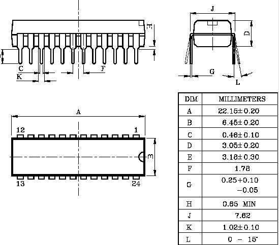
MMC1 comes in a 24 pin shrink-DIP package, .3" wide
MMC1 Pinout:
				  .---\/---.
		    PRG A14 (r) - |01    24| - +5V
		    PRG A15 (r) - |02    23| - M2
		    PRG A16 (r) - |03    22| - PRG A13 (s)
		    PRG A17 (r) - |04    21| - PRG A14 (n)
		    PRG /CE (r) - |05    20| - PRG /CE (n)
		    WRAM CE (w) - |06    19| - PRG D7 (s)
		    CHR A12 (r) - |07    18| - PRG D0 (s)
		    CHR A13 (r) - |08    17| - PRG R/W
		    CHR A14 (r) - |09    16| - CIRAM A10 (n)
		    CHR A15 (r) - |10    15| - CHR A12 (n)
		    CHR A16 (r) - |11    14| - CHR A11 (s)
			    GND - |12    13| - CHR A10 (s)
				  `--------'

				     MMC1

(r) - this pin connects to the ROM chips only
(n) - this pin connects to the NES connector only
(s) - this pin is shared with the NES connector and ROM chips
(w) - this pin connects to the WRAM only


Note: on some carts, several of the CHR ROM lines may be comondeered to run other functions,
such as 8K WRAM selection (SOROM) or PRG ROM A18 (SVROM I think?  Don't have a cart).
|

