Mapper 90 / Tekken 2
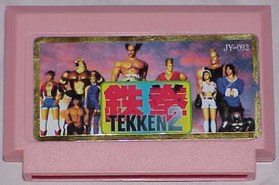
Cartridge Front
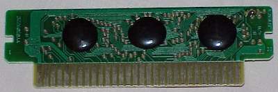
Cartridge Board
What Is It?
A strange "Tekken 2" original pirate. It has a somewhat-playable version of Tekken 2 on it. (Though, this same "fighting game engine" seems
to be used on most of the pirate fighting games from streetfighter to mortal kombat.)
The Tech:
This is the infamous "mapper 90". I finally reverse engineered it just about completely.
Using this information, Nintendulator can run all the mapper 90 games perfectly without ANY
hacks. I spent a fair amount of time figuring this information out.
Chip pinout, going in a clockwise circle.  from slightly left of
top dead center... the +5V connection.  There only appears to be
48 bondout pads, but there is no way of knowing how many are on
the chip itself.

1  - +5V
2  - PRG ROM A16 (r)
3  - PRG ROM A15 (r)
4  - PRG ROM A14 (r)
5  - PRG ROM A13 (r)
6  - /IRQ
7  - CHR /RD
8  - CHR ROM A18 (r)
9  - PRG R/W
10 - CHR ROM A17 (r)
11 - CHR ROM A16 (r)
12 - CHR ROM A15 (r)
13 - CHR ROM A14 (r)
14 - CHR ROM A13 (r)
15 - CHR ROM A12 (r)
16 - CHR ROM A11 (r)
17 - CHR ROM A10 (r)
18 - CIRAM /CE output (n)
19 - CHR A9 (s)
20 - CHR A8 (s)
21 - CHR A7 (s)
22 - CHR A6 (s)
23 - GND
24 - CHR A5 (s)
25 - CHR A4 (s)
26 - CHR A3 (s)
27 - CHR /A13 (n)
28 - CHR A12 (n)
29 - CHR A11 (n)
30 - CHR A10 (n)
31 - PRG D7 (s)
32 - PRG D6 (s)
33 - PRG D5 (s)
34 - PRG D4 (s)
35 - PRG D3 (s)
36 - PRG D2 (s)
37 - PRG D1 (s)
38 - PRG D0 (s)
39 - PRG ROM /CE (r)
40 - PRG A2 (s)
41 - PRG A1 (s)
42 - PRG A0 (s)
43 - PRG A14 (n)
44 - PRG A13 (n)
45 - PRG A12 (s)
46 - PRG /CE (n)
47 - CHR /RD (n)
48 - PRG M2 (n)


Register overview:
------------------

This mapper has ALOT of registers.  Fortunately, they are nicely broken up
by function.

All registers are selected using A0-A2, and A12-A15.


5000     : dipswitch register
5800-5FFF: multiplier/RAM byte(s) (see below)
8000-8003: PRG bank registers (note: 8004-8007 are mirrors)
9000-9007: CHR bank registers
A000-A007: CHR bank registers
B000-B007: nametable bank registers
C000-C007: IRQ registers
D000-D003: control registers (note: D004-D007 are mirrors)
E000-E007: unused
F000-F007: unused

I have cordoned off the registers according to function.  Without further
ado...

------------------------

PRG/CHR bankswitching:
-----

First, a word about banking.  All banks used are "Actual" banks.  This
means that if the bank size is 8K, the value written to the bank is the
ACTUAL bank.  i.e.  00h = first 8K, 01h = second 8K, etc.  This is true for
any bank size for both PRG and CHR.  There are no "dummy" bits in the lower
bit positions for larger banks like on most other mappers.

D000: Main bank size control register
-----


7       0
---------
MRNC CPPP


See the nametable control section for info on the R and N bits.

P: Program banking mode

M: Map in ROM at 6000-7FFF
0 - Don't map ROM
1 - map ROM

Below are the 8 PRG banking modes.  Note that the decoding done at 6000-7FFF
is only done when the M bit is set.  If it is not set, these addresses read
as open bus.

000b: (0)
-----
32K banks

6000-7FFF: last 8K of 32K bank selected by 8003
8000-FFFF: last 32K bank of ROM

001b: (1)
-----
16K banks

6000-7FFF: last 8K of 16K bank selected by 8003
8000-BFFF: 16K bank selected by 8001
C000-FFFF: last 32K of ROM

010b: (2)
-----
8K banks

6000-7FFF: 8K bank selected by 8003
8000-9FFF: 8K bank selected by 8000
A000-BFFF: 8K bank selected by 8001
C000-DFFF: 8K bank selected by 8002
E000-FFFF: last 8K bank of ROM

011b: (3)
-----
This works identically to the above, except it uses "bit reverse"
ordering (see below)

100b: (4)
-----
32K banks

6000-7FFF: last 8K of 32K bank selected by 8003
8000-FFFF: 32K bank selected by 8003

101b: (5)
-----
16K banks

6000-7FFF: last 8K of 16K bank selected by 8003
8000-BFFF: 16K bank selected by 8001
C000-FFFF: 16K bank selected by 8003

110b: (6)
-----
8K banks

6000-7FFF: 8K bank selected by 8003
8000-9FFF: 8K bank selected by 8000
A000-BFFF: 8K bank selected by 8001
C000-DFFF: 8K bank selected by 8002
E000-FFFF: 8K bank selected by 8003

111b: (7)
-----
Identical to the above, except used the "bit reverse" ordering (see below)


Bit reversing:
--------------
This mapper supports bit reversing for reasons unknown- possibly to make
routing PCBs easier since they have two ways to connect the address lines.
When this is used, D0 becomes D6, D1 becomes D5, etc.  D7 is not used
in any mode. I drew a little chart to make this easier to see:

7       0
---------
xABC DEFG  original bit order
xGFE DCBA  reversed bit order


----

Char bank control:

Registers 9000-9007 represent the 8 lower bits of the bank number
Registers A000-A007 represent the 8 upper bits of the bank number
Note: I do not know how many bank bits REALLY are present, however.

C:

00b: (0)
----
8K bank

0000-1FFF: 8K bank selected by 9000 & A000

01b: (1)
----
4K banks

0000-0FFF: 4K bank selected by 9000 & A000
1000-1FFF: 4K bank selected by 9004 & A004

10b: (2)
----
2K banks

0000-07FF: 2K bank selected by 9000 & A000
0800-0FFF: 2K bank selected by 9002 & A002
1000-17FF: 2K bank selected by 9004 & A004
1800-1FFF: 2K bank selected by 9006 & A006

11b: (3)
----
1K banks

0000-03FF: 1K bank selected by 9000 & A000
0400-07FF: 1K bank selected by 9001 & A001
0800-0BFF: 1K bank selected by 9002 & A002
0C00-0FFF: 1K bank selected by 9003 & A003
1000-13FF: 1K bank selected by 9004 & A004
1400-17FF: 1K bank selected by 9005 & A005
1800-1BFF: 1K bank selected by 9006 & A006
1C00-1FFF: 1K bank selected by 9007 & A007


D003:  CHR control register #1
-----

7       0
---------
DxEg gggG

gG bits:

These are the secondary bank control registers.

The bits in lower case have not been tested, because my cart only
contains 512K of CHR ROM.  I suspect they work similar to the G bits,
however.  The bits in these registers select a 256K CHR ROM bank when
the E bit is clear.  When the E bit is set, the normal banking registers
can select the entire space.

E: secondary CHR map register enable
0 - G bits control desired 256K CHR ROM bank
1 - G bits have no effect, and the entire CHR ROM is selected thru the
    main banking regs.

D: CHR bank mirror.
0 - normal operation
1 - CHR banks in the first 4K will be mirrored.

This bit is strange.  It only has an effect in 1K and 2K CHR ROM bank modes.
When in 1K mode, registers 9000 & A000 select a bank at 0000-03FF and at
0800-0BFFh.  Registers 9001 & A001 select a bank at 0400-07FF and at
0C00-0FFFh.  It appears to be some kind of address line disable or something.
I don't really know WHY it's here, but this is what it does!  This
probably doesn't have to be emulated, but I present it for completeness
sake.


D001:  CHR control register #2
-----

7       0
---------
xxxx xxMM


M: Mirroring bits:

00b (0) - Vertical
01b (1) - Horizontal
10b (2) - Nametable 0 only
11b (3) - Nametable 1 only


---------------------------------------------------


Nametable control
-----------------

This mapper has a fairly unique feature- it can actually map in CHR ROM
into the nametable space.  My cart (Tekken 2) did not allow this at first.
There were pads on the board and a spot for a resistor however which did.
When in the nametable control mode, a 1K resistor is put between CIRAM /CE
and CHR A13.  The mapper can then over-ride the /CE input to turn the RAM
off, and then the mapper can turn CHR ROM on.


Note: this is a board jumper selection.  Some (all?) games do not use this,
and enabling this mode always may cause problems with them.  The jumper allows
this mode to be enabled or disabled.

Anyways, it seems to be fairly straight forward.

(these bits are from register D000)

N: Nametable control enable
0 - disable nametable control (everything works like "normal", and NONE of the below applies)
1 - enable nametable control

R: When the above bit is enabled, then this bit is used:
0 - Nametables can either be RAM or ROM
1 - Nametables can be ROM only

Note: if bit N is clear, then bit R has no effect, and ROM data cannot be
mapped into nametable space.

D002:
-----

Bit 7 is the only bit of D002 that is used.  It only has an effect when
bit N is set and bit R is clear.


2000-23FF: 1K bank selected by B000 & B004
2400-27FF: 1K bank selected by B001 & B005
2800-2BFF: 1K bank selected by B002 & B006
2C00-2FFF: 1K bank selected by B003 & B007

B000-B003 is the lower 8 bits of the desired bank, while B004-B007 are the
upper bits.

When bit N is set and bit R is clear, the nametable RAM/ROM select mode is
enabled.  Bit 7 of B000-B003 will select between CHR ROM and RAM for each
nametable.

When bit 7 of the desired bank equals the bit value in D002 bit 7, RAM
is selected.  If they differ, ROM is selected.  Note that D7 of B000-B003
is still connected to the ROM.  D002 allows all 256K to be used (though,
all 4 nametables must use the same 128K bank).

D0 of the B000-B003 register selects a nametable when in the RAM mode.

------------------------------------------------


IRQ system
----------

IRQs on this mapper are insanely complex.  It involves 4 interrupt sources:

a) A12 toggles on PPU bus (For scanline counting)
b) M2 cycles
c) CPU writes.    Yes, CPU writes.  This sounds insane, but this is what
   the mapper is doing!  I verified it several ways.
d) PPU reads Yes, I verified this very thoroughly as well.

There is a prescaler, and a main IRQ counter.  The counters can count up
as well as down, depending on the bits in D001.

Here is a diagram of the insanity:


                             ---------------+
                       D0-D7 8              |
                             ----+   +--+   |
                                 |   |  | 8 |
                                 |   | +-----+
                                 |   | |     |
                                 |   | |latch|--o C006 write
                                 |   | +-----+
                                 | 8 |  | 8 |
                               +-------------+
                               |             |
                               |     XOR     |
                               +-------------+
                                 | 8 |
                                 |   +----------+
                                 |              |
                                 |   +------+   |
                                 |   |      |   |
            S bits     Dir.      \ 8 /      \ 8 /
             | |         |      +-----+    +-----+
             \ /         |      |     |    |     |
           +-----+    +-----+  U| Pre |   U|Main |
     M2 o--|0    |    |     |---|scale|----| Ctr |overflow
PPU A12 o--|1 Sel|----|demux|  D|     |   D|     |----------+
PPU /RD o--|2    |    |     |---|     |----|     |          |
CPU R/W o--|3    |    +-----+   |     |    |     |          |
           +-----+            +-|load |    |load |          |
                              | +-----+    +-----+          |
                    P bit o---+    |          |             |
                                   o          o             |
                              C004 write  C005 write        |
                                                            |
                                                            |
                                                            | IRQ latch
                                                         +--------+
                 +--+                +--+  IRQ en. FF    | ck     |
        D0 o-----|  |----------------|  |    +----+      |        |
              +--|& |  C003 write o--|or|----|S  Q|------|D     /Q|-o /IRQ
              |  +--+                +--+    |    |      |  R     |
C000 write o--o                              |    |      +--------+
              |  +--+                +--+    |    |         |
              +--|  |  C002 write o--|  |----|R /Q|---------+
       /D0 o-----|& |----------------|or|    +----+
                 +--+                +--+


C002: Disable interrupts
-----
Writing here will clear the IRQ flipflop and prevent further interrupts.
The value written is irrelevant.


C003: Enable interrupts
-----
Writing here will enable interrupts.  The value written is irrelevant.


C000: Alternate interrupt enable control register
-----

7       0
---------
xxxx xxxE

E: IRQ enable

0 - The same as writing to C002
1 - The same as writing to C003

I don't know why the IRQ functionality is duplicated like this.  Maybe to
make it compatible with 2 styles of mappers?  I can find no differences
between the method used to operate the IRQs.


C001: IRQ mode register
-----

7       0
---------
DUxx CPSS


S: IRQ counter source

00b (0) - M2 cycles
01b (1) - PPU A12 toggles
10b (2) - PPU reads
11b (3) - Writes to CPU space

Notes:  Yes, these IRQ sources look strange, particularly 2 and 3.
These have been extensively verified, however.  PPU reads would be a good
way to accomodate an exact position on the screen, with sub-scanline
accuracy.  CPU write counting could be used for complex copy protection
routines.

----

P: counter prescaler size

0 - prescaler is 8 bits (divide by 256)
1 - prescaler is 3 bits (divide by 8)

----

C: prescaler size adjust - related to C007

0 - Normal operation
1 - See C007 for more information about this odd mode.

Note: when this bit is set, the state of the P bit has no effect.

----

D: Count Down enable

0 - Don't count
1 - Each clock into the counter causes it to decrement by 1

U: Count Up enable

0 - Don't count
1 - Each clock into the counter causes it to increment by 1

Note:  If both the U and D bits are set or clear, the counter does not count.


C004: prescaler
-----

Writing here will load the prescaler with the value written XOR'd with the
value in C006.

C005: IRQ counter
-----

Writing here will load the IRQ counter with the value written XOR'd with
the value in C006.


C006: IRQ XOR register
-----

This value is XOR'd with C004/C005 when either of said addresses is written
to.  The value in C006 remains unchanged.  Most games seem to write 00h
here which effectively disables it.

C007:
-----

Prescaler size/enable. This register is odd.  It has no effect unless the
C bit of C001 is set.  If the C bit is set, then it behaves like so:

If any value but 0ffh is written to C007, the timer will not increment or
decrement.  If 0ffh is written, then the timer will operate, but the
prescaler will change.  I have have it be 12 instead of 8 sometimes, and
257 others.  There appears to be no rhyme or reason to it.  I tried alot
of things to get it back into the useful divide by 12 mode, but couldn't.
If a game uses this mode, I will reverse engineer it some more.  But since
no games use it, I will not bother.

IRQ Timer operation:
--------------------

The IRQ timer will expire after a specified number of clocks, firing off
an interrupt.  The method in which it does this has been exhaustively
checked using IRQ Master(tm) and CopyNES.  I wrote programs to count IRQ
cycles for around 500 thousand combinations to arrive at these formulas.


The timer is composed of two sub-timers.  The prescaler which can be
3 or 8 bits, and the timer itself which is 8 bits.

Here are the formulas for number of cycles to expiration:

---------------------
Select one:

For "down" counting:

upperbyte = C005 xor C006
lowerbyte = C004 xor C006

For "up" counting:

upperbyte = C005 xor C006 xor 0FFh
lowerbyte = C004 xor C006 xor 0FFh

---------------------
Select one:

for divide by 8:

total = ((upperbyte << 3) or (lowerbyte and 07h)) + 1

for divide by 256:

total = ((upperbyte << 8) or lowerbyte) + 1

---------------------

"total" is the *exact* number of clocks needed to fire an interrupt off.

----------------------------------------------------

5000: dipswitch / reading
-----

7       0
---------
DD00 0000

This allows you to read dipswitch settings.  Usually soldered pads on
the carts if they exist.  Many of the games will CHANGE DRAMATICALLY if
the upper bit is toggled on/off.  Tekken 2 turns into Toushinden, and
Aladdin turns into Aladdin 2, and MK3 Special 56 Pepoles changes into MK2!!

It seems that only D6 and D7 of this register are used. These 2 bits
are set by solderable jumpers on the cart.  This allows the game maker
to make identical carts for up to 4 "different" games.


Notes: the following registers were NOT implemented on my Tekken 2
cart, but this may only mean they are a chip bondout selection.
i.e. the A11 pad may just be grounded instead of connected to the
A11 line on the cart.  Some games rely on a multiplier and the RAM
byte being here for proper operation.

5800/5801: multiplier
----------

There is a multiplier here on some carts. The idea is you  write two
values here, wait 8 cycles, then read out 5800/5801 to get the result.

5800 will contain the lower 8 bits, while 5801 will contain the upper
8 bits.


5803: Single byte of RAM.
-----

This register is simply a byte of RAM, most likely to allow multicart
makers to remember the currently selected game.


5804: dunno
-----
Without a cart to test, I don't know if this mapper supports two bytes of RAM
down here, or possibly even 6 (5804-5807).  There isn't any way for me to test
without another cart.  Anyone got some they could spare?


----

Well, that about finishes up this bastard mapper.  Enjoy!
Oh yeah, here are some cool pictures I generated during reverse engineering.
On the X axis is register C005, on the Y axis is register C006. C004 was held at 00h
The colour indicates how long the IRQ took to fire, in counts.

When trying to reverse-engineer the C007 register, I got this out of the mapper. I don't
know exactly why it did what it did, but here it is anyways.

|